Single Layer PCB

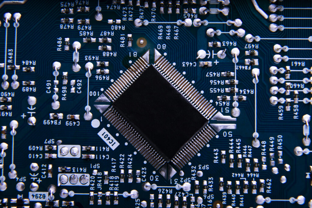
A single-layer PCB, also called a single-sided PCB, has one layer of conductive material (usually copper) on one side of an insulating substrate like fiberglass. Electronic components are placed on the opposite side and are connected to the copper traces through pads and vias. These PCBs are simple, cost-effective, and ideal for simple electronics like alarms, sensors, and power supplies. However, they have limited routing space and are not suitable for complex designs, and are more prone to crosstalk and interference.
A single-layer printed circuit board (PCB) is a type of PCB that has components and conductive tracks on only one side of the board. It is typically made of a non-conductive substrate, such as fiberglass or plastic, with a thin layer of metal, usually copper, applied to one side. The metal layer is then etched to create the desired circuit patterns and connections.
Key features
Construction
A single, non-conductive substrate with a single conductive layer of metal foil, most often copper, laminated to one side.
Components
All electronic components are placed on one side, and the conductive circuits (traces) are etched on the other side.
Protective layers
A solder mask is applied to protect the copper from oxidation and short circuits, and a silkscreen layer is often added for component labeling.
Design limitations
Circuits can only be laid out on one side, so conductive paths cannot overlap. This limits space and makes them less suitable for complex, high-density designs.
Interference
Due to the single layer, these boards are more susceptible to electromagnetic interference (EMI) and crosstalk compared to multi-layer boards, especially in sensitive applications.
